Tesla officially launched its Terafab chip manufacturing project on March 21, with seven new job postings confirming what had long been anticipated: the company intends to build its own domestic semiconductor fabrication facility. This isn’t a product announcement or a software update, it’s a structural shift in how Tesla plans to secure the compute it needs to scale FSD, Optimus, and everything in between.
The urgency behind Terafab isn’t subtle. Tesla has openly acknowledged that even its best-case supplier projections fall short of demand. Math is straightforward: 100 to 200 billion chips per year are required to support autonomous driving and humanoid robotics at scale. No external supplier can realistically meet that figure on Tesla’s timeline.
That constraint, projected to materialize within three to four years, is precisely what Terafab is designed to preempt. Austin is the starting point — hiring, planning, and site work are already underway, with full-volume production targeted for 2027 and beyond.
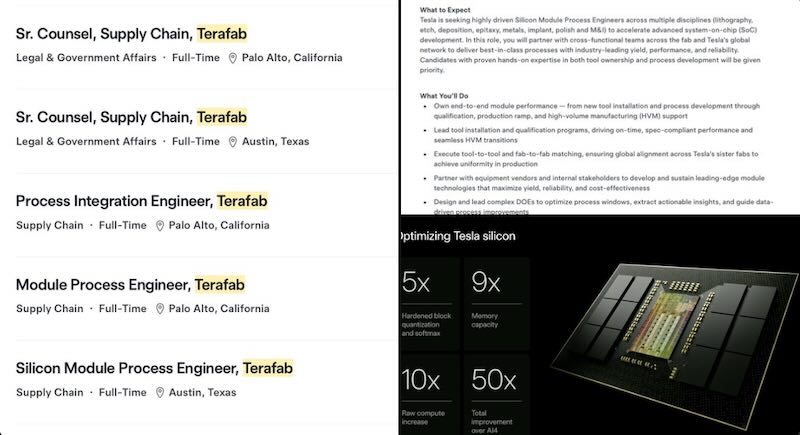
7 roles posted simultaneously signals a coordinated launch, not a exploratory phase. Positions span legal infrastructure, capital expenditure counsel, supply chain strategy, most critically process engineering.
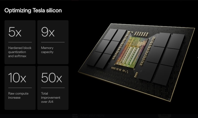
Tesla’s upcoming AI5 chip employs a half-reticle design strategy that could significantly reduce fabrication costs while maintaining performance targets. A reticle defines the imaging area used by lithography equipment during chip manufacturing, and fitting two chips per exposure effectively doubles production yield compared to single-reticle approaches.
Silicon Module Process Engineer listing is particularly telling. It prioritizes candidates with hands-on tool ownership and process development experience, targeting best-in-class yield, performance, and reliability. That’s not entry-level language. Tesla is recruiting for a facility it intends to operate at an industrial, competitive level.
Other postings including two separate Sr. Counsel, Supply Chain roles, reinforce that Terafab requires significant legal and operational scaffolding before a single chip is produced.
Marks the first time Tesla has used the word “Terafab” publicly in any official capacity. That alone signals a transition from internal planning to external commitment. Building a semiconductor fab is among the most capital-intensive undertakings in manufacturing, and Tesla is proceeding anyway.
For a company that has consistently brought critical supply chains in-house, from battery cells to motors, Terafab is the next logical step. Ambitious? Certainly. Expensive? Without question. But for Tesla, the chip may just be worth the fab.
Related Post
Tesla Restarts Dojo 3 Supercomputer After AI5 Chip Breakthrough
Tesla AI5 Chip Production Starts 2027: 40× Faster Performance, Elon Confirms Timeline
Rivian RAP1 Chip Powers New Gen 3 Autonomy Platform With Custom Silicon