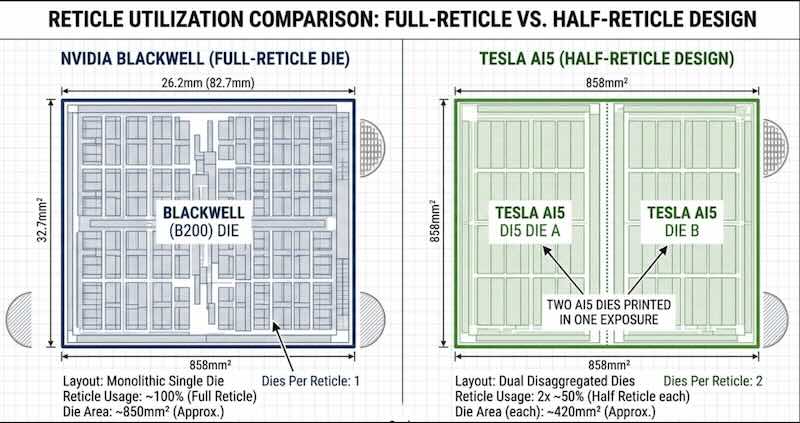
Tesla’s upcoming AI5 chip employs a half-reticle design strategy that could significantly reduce fabrication costs while maintaining performance targets. A reticle defines the imaging area used by lithography equipment during chip manufacturing, and fitting two chips per exposure effectively doubles production yield compared to single-reticle approaches.
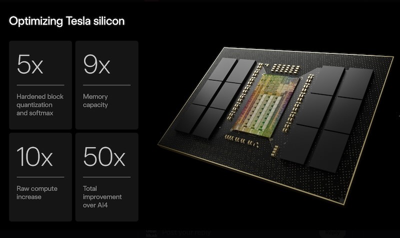
AI5 chip targets 250W power consumption, production delayed until 2027, Even after AI5 hardware begins appearing in Tesla vehicles in mid-2027, software that fully utilizes its capabilities likely won’t arrive until late 2027 or early 2028.
The design choice required Tesla’s chip engineering team to make strategic tradeoffs. The company removed older components including the image signal processor and traditional GPU to accommodate additional AI cores within the constrained space. Optimization reflects Tesla’s focus on inference workloads for edge computing applications rather than general-purpose processing.
NVIDIA’s Blackwell architecture occupies nearly a full reticle, representing a different set of priorities. Single-reticle design allows NVIDIA to maximize die area for datacenter-focused applications where performance density matters more than manufacturing efficiency.
Tesla’s half-reticle format positions the AI5 chip differently. If the company achieves its compute and efficiency objectives within this smaller footprint, the manufacturing requirements essentially get cut in half. Advantage compounds when Tesla scales production through its planned Terafab facility, particularly if subsequent generations like AI6 and AI7 maintain the half-reticle approach.
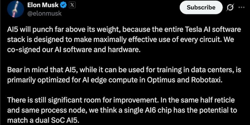
Elon Musk commented on the design philosophy behind the AI5 chip, stating it “will punch far above its weight, because the entire Tesla AI software stack is designed to make maximally effective use of every circuit. We co-designed our AI software and hardware.”
Chip targets edge computing deployments in Optimus humanoid robots and Robotaxi vehicles rather than traditional datacenter training workloads. Focus drives different design decisions than chips optimized primarily for cloud infrastructure.
Elon noted that while AI5 can handle training tasks in datacenters, its primary optimization centers on edge inference. He added that “there is still significant room for improvement. In the same half reticle and same process node, we think a single AI6 chip has the potential to match a dual SoC AI5.”
Statement suggests Tesla expects to deliver substantial performance improvements in future iterations without expanding the physical footprint. Achieving equivalent performance to two AI5 chips in a single AI6 chip would represent another doubling of efficiency.
Despite developing custom silicon, Elon emphasized that Tesla maintains its relationship with NVIDIA. “I am a huge admirer of Nvidia and Jensen btw. That market cap is well-deserved. SpaceX AI and Tesla expect to continue ordering Nvidia chips at scale.”
AI5 chip demonstrates how Tesla’s vertical integration extends beyond vehicles into semiconductor design, with manufacturing efficiency baked into the architecture from the start.
Related Post
Tesla AI5 Chip Production Starts 2027: 40× Faster Performance, Elon Confirms Timeline
Tesla Restarts Dojo 3 Supercomputer After AI5 Chip Breakthrough
Tesla Giga Texas Cortex 2: 500MW GPU Cluster Coming Mid-2026